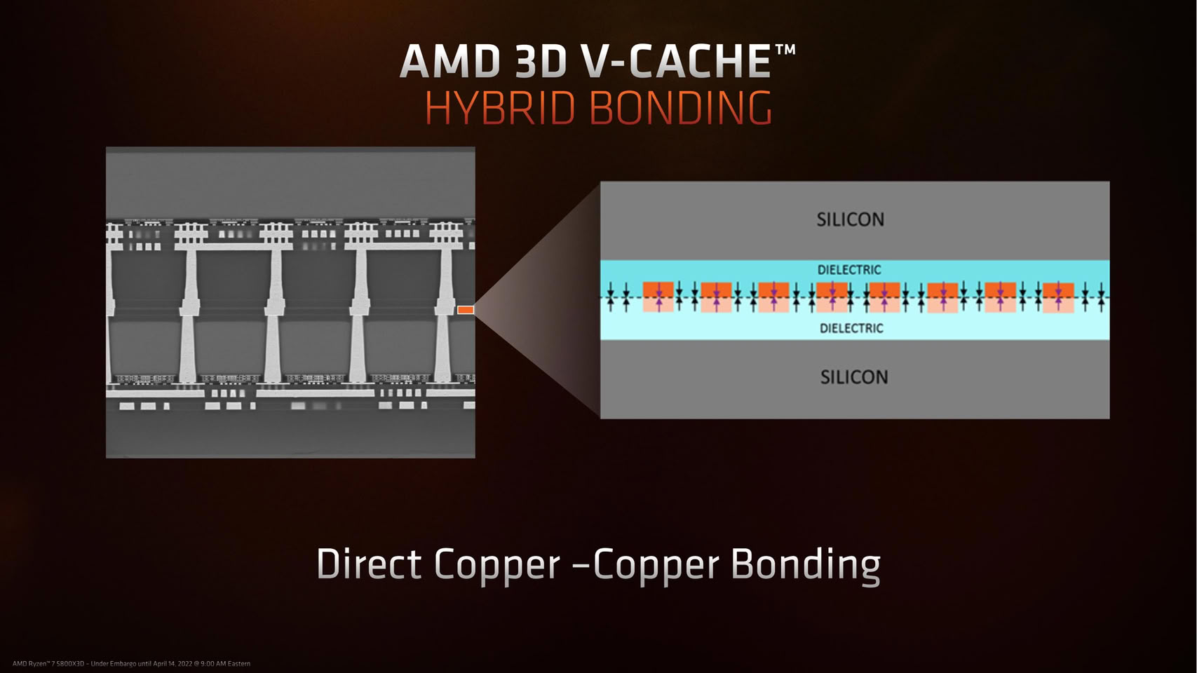
According to the latest report from ETNews, citing supply chain . For those unfamiliar, hybrid bonding creates a permanent bond between two silicon chips using embedded metal bumps that are fused together to form a single chip. Multiple dies or entire silicon wafers can be connected by stacking the back ends of two chips together.
This technology eliminates traditional chip bumps and directly bonds copper interconnections between the two chips. In modern packaging, chip solder bumps, which stick out before the chip is soldered to the PCB, are roughly 100 micrometers in size, while microbumps are approximately 20 micrometers.
Hybrid bonding reduces this size to 1 micrometer. Microbumps are used to interconnect silicon with other chips inside a package, as seen in CoWoS-S and CoWoS-L, where microbumps are prevalent for chip-to-interposer connections. For TSMC, the future may involve bypassing hybrid bonding technology and investing in microbumps that are 5 micrometers in size.
Reportedly, TSMC is preparing its supply chain for 5-micrometer microbumps, which will be even smaller than what is currently available, to enhance performance in packaging. South Korean and Japanese suppliers are reportedly collaborating with TSMC to achieve this, with mass production of 5-micrometer microbumps expected in the second half of 2028.
As a reminder, AMD's 3D V-Cache technology uses hybrid bonding to put SRAM on top of logic, but TSMC only has limited production capacity of that for now, which will remain limited seemingly. Read full story